4-Bit Adder Project Report
made by eng. Abderhman Waled Abdelkareem:
Understanding the 4-Bit Adder
A 4-bit adder is a digital circuit designed to add two 4-bit binary numbers. It produces a 4-bit sum output and a carry-out bit to indicate overflow beyond the 4 bits. This adder forms a vital part of the arithmetic logic unit (ALU) found in most digital processing systems, enabling fundamental arithmetic operations.

the main logic building block of the project (full adder)
Circuit Design and Structure
The 4-bit adder circuit is constructed by linking four full-adder units in series. Each full adder is responsible for adding corresponding bits from both input numbers along with the carry-in from the previous stage.
Each full adder employs several logic gates:
- XOR gates
- AND gates
- OR gates

the full logic diagram of the project
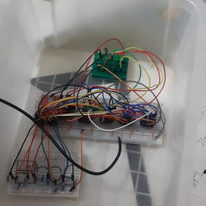
Components and Assembly
The 4-bit adder project relies on several integrated circuits (ICs) and discrete components for construction and testing. The primary ICs include:
- 74HC86: Quad 2-input XOR gates used to generate sum outputs for each bit.
- 74HC08: Quad 2-input AND gates employed in producing intermediate carry signals.
- 74HC32: Quad 2-input OR gates used for final carry-out calculations.
Complementing these are practical assembly materials:
- Breadboards for physical prototyping without soldering.
- Jumper wires for making reliable electrical connections.
- 1kΩ resistors to ensuring stable inputs (AVOID floating).
- Green LEDs acting as output indicators to visualize the sum and carry bits.
- Two 4-way DIP switches providing manual binary input entry for the two 4-bit numbers.

the chip used for XOR gate is:74HC86 which is 4 gates in one chip

the chip used for OR gate is:74HC32 which is 4 gates in one chip

the chip used for AND gate is:74HC08 which is 4 gates in one chip
Internal Structure of IC Chips
Chip | Function | Internal Composition |
74HC86 | Quad 2-input XOR Gates | Four XOR gates with MOSFET transistors |
74HC08 | Quad 2-input AND Gates | Four AND gates with MOSFET transistors |
74HC32 | Quad 2-input OR Gates | Four OR gates with MOSFET transistors |


Lessons Learned and Challenges Encountered
Key Learnings:
- Understanding Logic Gates: I learned how XOR, AND, and OR gates function and how they can be combined to form complex logic like a full adder.
- Binary Addition: Gained a clear understanding of how binary numbers are added bit by bit and how carry propagation works.
- TTL vs CMOS Compatibility: Faced issues with voltage compatibility. CMOS outputs (like 74HC series) may not reliably trigger TTL inputs if not properly interfaced. This required verifying that voltage levels were within acceptable limits.
- Floating Inputs: I discovered that floating logic inputs can cause unpredictable behavior. Pull-down or pull-up resistors are necessary to ensure known default states.
- Electrical Circuit Design: Gained practical experience in designing and troubleshooting a digital logic circuit, including power management, grounding, and using DIP switches effectively.
Problems Encountered:
- Voltage Level Issues: The output from the CMOS logic gates was sometimes not high enough to be recognized as a logical "1" by TTL devices. I had to make sure all components were from the same family or had compatible logic levels.
- Unstable Outputs: Due to floating inputs or poor connections, the LEDs sometimes flickered. This was solved by adding pull-down resistors and ensuring solid jumper wire connections.