I decided to jump headfirst into something completely new: a 24-hour hands-on FPGA course spread over just 6 days. Here’s the twist — I had never studied logic design or computer architecture before. My only prior experience was building a simple 4-bit adder as a hardware project. So, enrolling in an FPGA course wasn’t just a step forward… it was a leap. The course focused on using Xilinx Vivado and VHDL to design digital systems and testing on a Xilinx PYNQ-Z2 board. It was an intense mix of coding, simulation, and hardware testing — and I learned a lot more than I expected. In this blog, I’ll take you through that experience and what it was like diving into the deep end of FPGA development.

Xilinx PYNQ-Z2 board
After hearing about my spontaneous dive into FPGA, people often have one of two reactions. One group questions my decision: "Why would you take this if you've never studied logic design or computer architecture?" The other jumps straight to curiosity: "What even is an FPGA?" This section aims to address both those questions
What is an FPGA?
In my terms, an FPGA is like a artist’s blank canvas. Instead of painting with colors, you 'paint' with logic gates. It’s a piece of hardware you can reconfigure to become almost any digital circuit you can imagine
also —>
A field-programmable gate array (FPGA) is a type of configurable integrated circuit that can be repeatedly programmed after manufacturing. FPGAs are a subset of logic devices referred to as programmable logic devices (PLDs). They consist of a grid-connected array of programmable logic blocks that can be configured 'in the field' to interconnect with other logic blocks to perform various digital functions.
— Wikipedia
Why Did I Take the Course?
Simple: I love a challenge. I love when people doubt me, and I get to prove them wrong. also, My only hardware experience before this was building a small 4-bit adder — and I enjoyed it so much that I wanted to see what would happen if I took that curiosity to the next level. FPGA felt like the perfect playground for that.
Hands-On FPGA
Over the 6 days, the course packed a lot of hands-on work into a short time. Almost every session was about building something in VHDL using Vivado, running simulations. Here’s a quick rundown of the main things I worked on:
4-Bit Adder
My first task was to code a simple 4-bit adder in VHDL, run it through Vivado, and verify it with simulation.
Decoder Design & Simulation
Next, I wrote a decoder in VHDL, again testing it with simulation to ensure it behaved as expected.
Mini ALU Development
We started building a small Arithmetic Logic Unit. (I’ll go into more detail about this later — it was one of my favorite parts.)
Flip-Flops
Learned about flip-flops and how to use them in designs.
Synchronous vs. Asynchronous Logic ,Sequential vs. Combinational
Understood the core differences between these design styles and when to use each.
Vivado Core Generator Exploration
Explored Vivado’s built-in core generator to create reusable, pre-optimized components.
FIR Filter Implementation
Wrote a Finite Impulse Response (FIR) filter in VHDL and simulated its behavior.
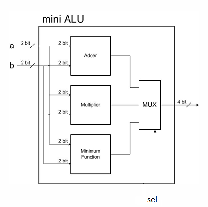
The mini ALU
As promised, here’s the breakdown of the mini ALU: We start with two 2-bit inputs. These first pass through flip-flops, then go into three different units — an adder, a multiplier, and a subtractor. Each of these produces its own output. All three outputs are then fed into a multiplexer. A 2-bit selection input chooses which one of these results becomes the final 4-bit output. You can see the whole flow in the diagram below
THE CODE
library IEEE;
use IEEE.STD_LOGIC_1164.ALL;
use IEEE.NUMERIC_STD.ALL;

entity alu_2bit is
    Port (
        clk     : in  STD_LOGIC;
        a       : in  STD_LOGIC_VECTOR(1 downto 0);
        b       : in  STD_LOGIC_VECTOR(1 downto 0);
        sel     : in  STD_LOGIC_VECTOR(1 downto 0);
        result  : out STD_LOGIC_VECTOR(3 downto 0)
);
end alu_2bit;

architecture Behavioral of alu_2bit is

    signal a_reg   : STD_LOGIC_VECTOR(1 downto 0);
    signal b_reg   : STD_LOGIC_VECTOR(1 downto 0);
    signal sel_reg : STD_LOGIC_VECTOR(1 downto 0);
    signal result_reg : STD_LOGIC_VECTOR(3 downto 0);

    signal a_int   : unsigned(1 downto 0);
    signal b_int   : unsigned(1 downto 0);


begin


    a_int <= unsigned(a_reg);
    b_int <= unsigned(b_reg);
    process(clk)
    begin
        if rising_edge(clk) then
            a_reg   <= a;
            b_reg   <= b;
            sel_reg <= sel;
            case sel_reg is
                when "00" => result_reg <= std_logic_vector(resize(a_int, 4) + resize(b_int, 4));
                when "01" => result_reg <= std_logic_vector(resize(a_int, 4) * resize(b_int, 4));
                when "10" => result_reg <= std_logic_vector(resize(a_int, 4) - resize(b_int, 4));
                when others => result_reg <= "0000";
            end case;
        end if;
    end process;
    result <= result_reg;
end Behavioral;
Simulating the Mini ALU:
Here’s a screenshot of the waveform simulation. For this run, I used ModelSim instead of Vivado — that way, I’ve now tried both programs.

Challenges I faced while writing this code:
ModelSim Error Identification
Unlike Vivado, ModelSim doesn’t directly point to where the error is, so I had to guess multiple times until I found the problem.
Clock and Flip-Flop Management
Making sure the clock signal and flip-flops were handled correctly took careful adjustment.
Arithmetic Library Selection
I needed the correct libraries to use the +, -, and * operators.
Bit Resizing for Operations
I had to resize signals so that arithmetic operations could work properly.
Output Synchronization via Flip-Flops (over flow error)
To prevent overflow issues, I used flip-flops to store intermediate results.